|


 |
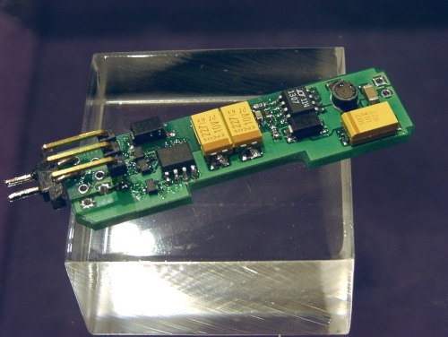
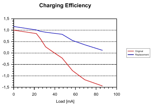
The replacement converter circuitDesigning a replacement circuit meant starting from the very beginning as the original components are no longer available. The goal was to design a drop-in replacement working with the same AC adapter and providing the same functionality. It copies the achitecture of the TL496 circuit and is based on an LT1307 switch-mode controller from Linear Technology (see datasheet). An extra linear regulator allows operating the calculator from adapter power. The result is the circuit board shown below: The picture is a BP-7 replacement board. BP-8 and BP-9 are essentially the same, but they have a different DC output connector. Circuit comparisonWhen it comes to comparing performance of both circuits, which one does better? Well, this is somewhat unfair because there are twenty years of electronic innovation in between. But keeping this in mind, the original circuit does an excellent job. No power supply chip of today can provide this functionality with only four external components. But lets look into the details: Output voltage qualityWhen accumulator-powered, the original circuit generates a train of huge spikes at the output, reaching 14 V. This is not only an EMC issue, but it would most likely kill many more recent circuits supplied by it. This is due to the high ESR of the electrolytic storage capacitor, resulting in bad high frequency noise suppression. The new circuit switches at a much higher frequency and has better filtering at the input and output, so the output voltage is very quiet. Conversion efficiencyThe original circuit is said to have an efficiency of 66%. The new circuit has an efficiency of 76% at full load, making it draw 13% less current from the accumulators. Charging efficiencyAs mentioned before, putting heavy load on the original circuit while it charges the accumulators results in reduced charging efficiency and may
even discharge them. This effect is much less pronounced in the replacement circuit, as is shown in the following graph. Positive values mean charging, negative values mean discharging. All values are
normalized to original circuit efficiency at no load. The original circuit has a turnaround point at about 40 mA of load current at which accumulators begin to discharge. Not only is overall charging efficiency of the new circuit much better, but it never becomes negative, not even at full load. Idle CurrentThe output capacitor has some leakage current the voltage converter has to compensate. So, even with the calculator turned off, the converter recharges the capacitor once every few seconds. Together with the quiescent current of the chip, the original circuit draws about 120-190 µA from the accumulator, while the replacement circuit draws 155 µA. Run and recharge timesUsing medium capacity cells (1500 mAh) with the new circuit, the following times can be achieved:
|